Technology support for your microsystem.
What we offer
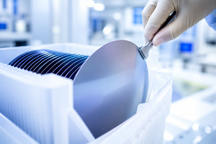
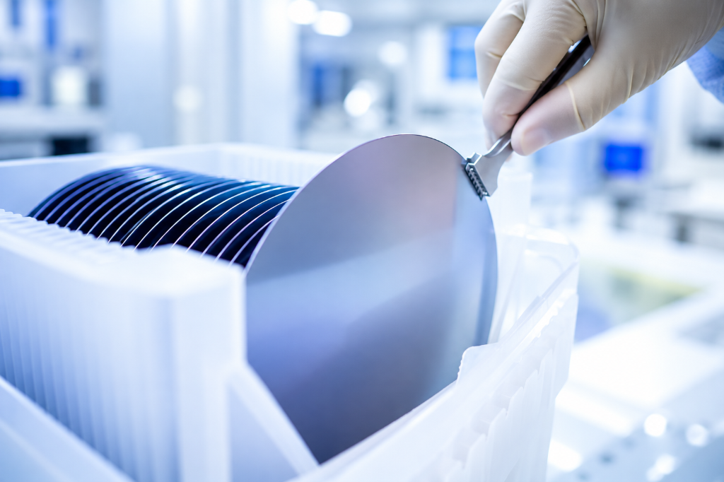
Our range of services includes established methods of microtechnology such as UV lithography, plasma etching, plasma coating, thin film technology, wet chemical processes as well as other manufacturing technologies for structuring, deposition, and processing of 100 mm and 200 mm wafers.
Our focus is on the technological implementation of your microsystem. For this purpose, we specifically provide you with our design & process expertise.
This gives you easy access to MEMS design and manufacturing technologies – flexible for prototypes, development work, small series, and individual processing tasks.
Depending on the requirements, we take on both individual technological process steps up to prototyping.
UV-
lithography
100 mm or 200 mm wafer technology
thin film technology
Sputtering (Al, Cr, Ti, Ni, Pt, Mo)
Reactive sputtering (AlN, TiN)
Evaporation (Au, Ni, Cr, Mo, Ti)
Plasma
etching &
coating
RIE, DRIE, PECVD
Analytics
Microscopy (confocal microscopy, SEM, light microscopy)
Profilometry
Ellipsometry
Individual processes & prototyping
Do you only need a single process step or do you want to manufacture a complete microsystem? We offer flexible manufacturing solutions based on 100 mm and 200 mm wafer technology.
Request a quote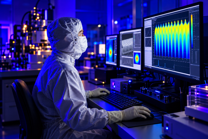
Mask service
We transfer your chip design into a production-ready mask layout and deliver the appropriate masks directly to you.

MEMS design support
Do you want to develop a microsystem? We support you from the first design idea to the technical elaboration. With solid MEMS design support, FE simulations, and process planning, we help you turn your project into reality.